- 您现在的位置:买卖IC网 > Sheet目录514 > SIA461DJ-T1-GE3 (Vishay Siliconix)MOSFET P-CH 20V 12A SC706L
�� �
�
�New� Product�
�SiA461DJ�
�Vishay� Siliconix�
�P-Channel� 20-V� (D-S)� MOSFET�
�FEATURES�
�PRODUCT� SUMMARY�
�?� TrenchFET� ?� Power� MOSFET�
�V� DS� (V)�
�-� 20�
�R� DS(on)� (� ?� )� Max.�
�0.033� at� V� GS� =� -� 4.5� V�
�0.042� at� V� GS� =� -� 2.5� V�
�0.055� at� V� GS� =� -� 1.8� V�
�I� D� (A)� a�
�-� 12�
�-� 12�
�-� 12�
�Q� g� (Typ.)�
�18� nC�
�?� Thermally� Enhanced� PowerPAK� ?� SC-70� Package�
�-� Small� Footprint� Area�
�-� Low� On-Resistance�
�?� Material� categorization:�
�For� definitions� of� compliance� please� see�
�www.vishay.com/doc?99912�
�APPLICATIONS�
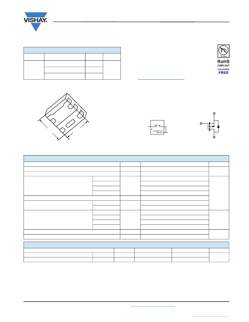
�PowerPAK� SC-70-6L-Sin� g� le�
�?� Smart� Phones,� Tablet� PCs,� Mobile� Computing�
�-� Battery� Switch�
�-� Charger� Switch�
�D�
�1�
�D�
�2�
�3�
�-� Load� Switch�
�(4)� S�
�6�
�D�
�G�
�Markin� g� Code�
�5�
�D�
�S�
�Part� #� code�
�B� V� X�
�(3)� G�
�2.05� mm�
�4�
�S�
�2.05� mm�
�XXXX�
�Lot� Tracea� b� ility�
�and� Date� code�
�(1,� 2,� 5,� 6)� D�
�Orderin� g� Information:�
�SiA461DJ-T1-GE3� (Lead� (P� b� )-free� and� Halogen� free)�
�ABSOLUTE� MAXIMUM� RATINGS� (T� A� =� 25� °C,� unless� otherwise� noted)�
�P-Channel� MOSFET�
�Parameter�
�Drain-Source� Voltage�
�Gate-Source� Voltage�
�T� C� =� 25� °C�
�Symbol�
�V� DS�
�V� GS�
�Limit�
�-� 20�
�±8�
�-� 12� a�
�Unit�
�V�
�Continuous� Drain� Current� (T� J� =� 150� °C)�
�Pulsed� Drain� Current� (t� =� 300� μs)�
�Continuous� Source-Drain� Diode� Current�
�T� C� =� 70� °C�
�T� A� =� 25� °C�
�T� A� =� 70� °C�
�T� C� =� 25� °C�
�T� A� =� 25� °C�
�T� C� =� 25� °C�
�I� D�
�I� DM�
�I� S�
�-� 12� a�
�-� 8.3� b,� c�
�-� 6.6� b,� c�
�-� 20�
�-� 12� a�
�-� 2.8� b,� c�
�17.9�
�A�
�Maximum� Power� Dissipation�
�T� C� =� 70� °C�
�T� A� =� 25� °C�
�P� D�
�11.4�
�3.4� b,� c�
�W�
�T� A� =� 70� °C�
�2.2� b,� c�
�Operating� Junction� and� Storage� Temperature� Range�
�Soldering� Recommendations� (Peak� Temperature)� d,� e�
�T� J� ,� T� stg�
�-� 55� to� 150�
�260�
�°C�
�THERMAL� RESISTANCE� RATINGS�
�Parameter�
�Symbol� Typical� Maximum� Unit�
�Maximum� Junction-to-Ambient� b,� f�
�Maximum� Junction-to-Case� (Drain)�
�t� ?� 5s�
�Steady� State�
�R� thJA�
�R� thJC�
�29� 37�
�5.5� 7�
�°C/W�
�Notes:�
�a.� Package� limited.�
�b.� Surface� mounted� on� 1"� x� 1"� FR4� board.�
�c.� t� =� 5� s.�
�d.� See� solder� profile� (www.vishay.com/doc?73257).� The� PowerPAK� SC-70� is� a� leadless� package.� The� end� of� the� lead� terminal� is� exposed� copper�
�(not� plated)� as� a� result� of� the� singulation� process� in� manufacturing.� A� solder� fillet� at� the� exposed� copper� tip� cannot� be� guaranteed� and� is� not�
�required� to� ensure� adequate� bottom� side� solder� interconnection.�
�e.� Rework� conditions:� manual� soldering� with� a� soldering� iron� is� not� recommended� for� leadless� components.�
�f.� Maximum� under� steady� state� conditions� is� 80� °C/W.�
�Document� Number:� 63838�
�S12-0539-Rev.� A,� 12-Mar-12�
�For� more� information� please� contact:� pmostechsupport@vishay.com�
�www.vishay.com�
�1�
�This� document� is� subject� to� change� without� notice.�
�THE� PRODUCTS� DESCRIBED� HEREIN� AND� THIS� DOCUMENT� ARE� SUBJECT� TO� SPECIFIC� DISCLAIMERS,� SET� FORTH� AT� www.vishay.com/doc?91000�
�发布紧急采购,3分钟左右您将得到回复。
相关PDF资料
SIA511DJ-T1-GE3
MOSFET N/P-CH 12V PWRPAK SC70-6
SIA513DJ-T1-GE3
MOSFET N/P-CH 20V PWRPAK SC70-6
SIA533EDJ-T1-GE3
MOSFET N/P-CH 12V 4.5A SC70-6
SIA777EDJ-T1-GE3
MOSFET N/P-CH 20V PPAK SC70-6L
SIA811DJ-T1-GE3
MOSFET P-CH 20V 4.5A SC70-6
SIA814DJ-T1-GE3
MOSFET N-CH 30V 4.5A SC70-6
SIA911EDJ-T1-GE3
MOSFET P-CH DL 20V PWRPAK SC70-6
SIA914DJ-T1-GE3
MOSFET DL N-CH 20V PPAK SC70-6
相关代理商/技术参数
SIA462DJ-T1-GE3
制造商:Vishay Semiconductors 功能描述:MOSFETS - Tape and Reel 制造商:Vishay Intertechnologies 功能描述:MOSFET 30V 18mOhm@10V 12A N-Ch 制造商:Vishay Intertechnologies 功能描述:N-CHANNEL 30-V (D-S) MOSFET
SIA467EDJ
制造商:VISHAY 制造商全称:Vishay Siliconix 功能描述:P-Channel 12 V (D-S) MOSFET
SiA467EDJ-T1-GE3
功能描述:MOSFET -12V .013Ohm@4.5V 31A P-Ch G-III
RoHS:否 制造商:STMicroelectronics 晶体管极性:N-Channel 汲极/源极击穿电压:650 V 闸/源击穿电压:25 V 漏极连续电流:130 A 电阻汲极/源极 RDS(导通):0.014 Ohms 配置:Single 最大工作温度: 安装风格:Through Hole 封装 / 箱体:Max247 封装:Tube
SIA477EDJ-T1-GE3
功能描述:MOSFET 12V 14mOhm@4.5V 12A P-Ch
RoHS:否 制造商:STMicroelectronics 晶体管极性:N-Channel 汲极/源极击穿电压:650 V 闸/源击穿电压:25 V 漏极连续电流:130 A 电阻汲极/源极 RDS(导通):0.014 Ohms 配置:Single 最大工作温度: 安装风格:Through Hole 封装 / 箱体:Max247 封装:Tube
SIA483DJ
制造商:VISHAY 制造商全称:Vishay Siliconix 功能描述:P-Channel 30 V (D-S) MOSFET
SIA483DJ-T1-GE3
功能描述:MOSFET -30V 21mOhm@10V 12A P-Ch G-III
RoHS:否 制造商:STMicroelectronics 晶体管极性:N-Channel 汲极/源极击穿电压:650 V 闸/源击穿电压:25 V 漏极连续电流:130 A 电阻汲极/源极 RDS(导通):0.014 Ohms 配置:Single 最大工作温度: 安装风格:Through Hole 封装 / 箱体:Max247 封装:Tube
SIA511DJ
制造商:VISHAY 制造商全称:Vishay Siliconix 功能描述:N- and P-Channel 12-V (D-S) MOSFET
SIA511DJ-T1-E3
功能描述:MOSFET 12V 4.5A 6.5W RoHS:否 制造商:STMicroelectronics 晶体管极性:N-Channel 汲极/源极击穿电压:650 V 闸/源击穿电压:25 V 漏极连续电流:130 A 电阻汲极/源极 RDS(导通):0.014 Ohms 配置:Single 最大工作温度: 安装风格:Through Hole 封装 / 箱体:Max247 封装:Tube